البريد الالكتروني:[email protected]
silicon wafer backgrinding process
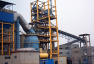
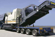
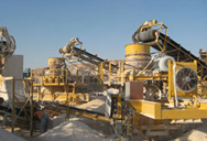
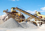
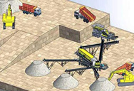
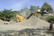
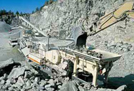
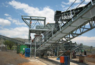
الشركة المصنعة أساسا الكسارات المتنقلة، كسارات ثابتة، آلات صنع الرمل، والطواحين والمصانع الكاملة التي يتم استخدامها على نطاق واسع في مجال التعدين، والبناء، والطرق السريعة والجسور والفحم والكيماويات والمعادن، والمواد المقاومة للحرارة، الخ جودة المنتج هو الحياة، و الابتكار العلمي هو القوة المحركة. لي منغ حصلت ISO شهادة نظام الجودة الدولية، شهادة الاتحاد الأوروبي CE وشهادة GOST الروسي. والشركة لديها البحث والتطوير القوي قوة والابتكار.
-
-
Wafer Backgrinding Services Silicon Wafer Thinning
2021-6-20 The backgrinding process involves using a diamond-resin bonded grinding wheel to remove the silicon material from the back of a silicon wafer. Using a grinding wheel is highly effective, and faster and less expensive than chemical-mechanical
دردشة على الإنترنت Read More -
-
Backgrinding - Desert Silicon
Backgrinding is the process of removal of silicon from the back of wafers following conventional semiconductor processing. The process is primarily utilized in thinning wafers for commercial semiconductor wafer fabs. Wafers are first laminated using an automatic taping machine.
دردشة على الإنترنت Read More -
-
Warping of silicon wafers subjected to back-grinding
2015-4-1 The grinding-based back-thinning process is featured with a rotating wafer which is held by a vacuum chuck,. The wafer is induced with stresses by grinding which are partially released when the wafer is removed from the chuck. Residual stresses are thus left in the ground wafer.
دردشة على الإنترنت Read More -
-
The back-end process: Step 3 – Wafer backgrinding ...
The Backgrinding Process . To improve the productivity of an operation, a multi-step grinding operation is generally performed. The first step uses a large grit to coarsely grind the wafer and remove the bulk of the excess wafer thickness.
دردشة على الإنترنت Read More -

-
Fine grinding of silicon wafers - K-State
2006-5-21 Besides being a major flattening process, surface grinding has also been proposed to replace etching [5], even for producing 400 mm silicon wafers [6]. In addition to its applications in silicon wafer manufacturing, surface grinding has also been used for “backgrinding”. In backgrinding, silicon wafers containing completed devices on their
دردشة على الإنترنت Read More -
-
Wafer Backgrind - EESemi
2019-8-14 Wafer Backgrind. Wafer Backgrind. Wafer Backgrind is the process of grinding the backside of the wafer to the correct wafer thickness prior to assembly. It is also referred to as 'wafer thinning.'. Wafer backgrinding has not always been
دردشة على الإنترنت Read More -
-
Wafer Backgrind - AnySilicon Semipedia
Wafer backgriding is a process of thinning the wafer to meet the required thickness before packaging the die into its package. Wafer backgrinding is also called wafer thinning or wafer back-lapping. Backgrinding process is not a mandatory step in ASIC production, however, thinner semiconductor packages has made it
دردشة على الإنترنت Read More -

-
Semiconductor Back-Grinding - idc-online
2019-2-4 Grinding is a complex process, and Figure 2 illustrates the parameters for a three-pass grinding operation. Lewis ground wafers to constant thickness under different conditions and then, using a three-point bend test mechanism, measured the break strength of dice from different locations on the wafer. His findings were consistent with the theory that, since silicon behaves much like glass, grinding
دردشة على الإنترنت Read More -
-
Silicon Wafer Thinning, the Singulation Process, and Die ...
2018-11-29 During front-end production of semiconductor devices, electronic circuits such as transistors are formed on the surface of a silicon wafer. Subsequently, in back-end production, the wafer backside is thinned and the wafer is singulated by dicing. The chips are then encapsulated in a package that will be delivered to end-users. The need for thinner chips has been growing in recent years to support lower
دردشة على الإنترنت Read More -
-
Warping of silicon wafers subjected to back-grinding
2015-4-1 This study investigates warping of silicon wafers in ultra-precision grinding-based back-thinning process. By analyzing the interactions between the wafer and the vacuum chuck, together with the machining stress distributions in damage layer of ground wafer, the study establishes a mathematical model to describe wafer warping during the thinning process using the elasticity theory.
دردشة على الإنترنت Read More -
-
Wafer Backgrind - EESemi
2019-8-14 Wafer Backgrind Wafer Backgrind is the process of grinding the backside of the wafer to the correct wafer thickness prior to assembly. It is also referred to as 'wafer thinning.' Wafer backgrinding has not always been necessary, but the drive to make packages thinner and thinner has made it
دردشة على الإنترنت Read More -
-
Warping of silicon wafers subjected to back-grinding
This study investigates warping of silicon wafers in ultra-precision grinding-based back-thinning process. By analyzing the interactions between the wafer and the vacuum chuck, together with the machining stress distributions in damage layer of ground wafer, the study establishes a mathematical model to describe wafer warping during the thinning process using the elasticity theory.
دردشة على الإنترنت Read More -
-
Wafer Backgrind - AnySilicon Semipedia
Wafer Backgrind. Wafer backgriding is a process of thinning the wafer to meet the required thickness before packaging the die into its package. Wafer backgrinding is also called wafer thinning or wafer back-lapping. Backgrinding process is not a mandatory step in ASIC production, however, thinner semiconductor packages has made it unavoidable.
دردشة على الإنترنت Read More -
-
A Study of Wafer Backgrinding Tape Selection for SOI
2019-11-26 22 responsible for grinding the silicon die to its thickness is wafer backgrinding. As a major 23 preliminary process at the back end, one of its sub-processes is the wafer preparation prior 24 grinding wherein silicon wafer is been taped on the active layer to protect it from any 25 contaminants and water penetration during the grinding ...
دردشة على الإنترنت Read More -
-
Semiconductor Back-Grinding - idc-online
2019-2-4 The silicon wafer on which the active elements are created is a thin circular disc, typically 150mm or 200mm in diameter. During diffusion and similar processes, the wafer may become bowed, but wafers for assembly are normally stress relieved and can be regarded as flat. Frequently there will be a departure from roundness, with a flat or notch
دردشة على الإنترنت Read More -
-
Wafer Backgrinding and Semiconductor Thickness
Wafer backgrinding is the first step in semiconductor packaging, the process of encasing one or more discrete semiconductor devices or integrated circuits (IC) for protection. Known also as wafer thinning or wafer lapping, backgrinding reduces wafer thickness to allow stacking and high-density IC packaging.
دردشة على الإنترنت Read More -
-
Backgrinding Tape Selection Analysis for Adhesion
2019-11-26 77 2.1 Wafer Backgrinding Process 78 79 Wafer back grinding is the thinning of semiconductor wafers by removing material from the 80 unpolished wafer back side. Wafers are often fabricated thicker than necessary, normally at 81 600 to 750µm thick, and this has been determined by the stresses during processing and the
دردشة على الإنترنت Read More -
-
NOVEL ULTRAFILTRATION OPERATING PROCESS FOR
2019-1-7 PROCESS FOR SILICON WAFER PRODUCTION WASTEWATER REUSE Ben Freeman Hydranautics – A Nitto Group Company ... * Assumes production of single 300 mm silicon wafer requires ~2000 gallons of water. Source: Sage Concepts Market Report . ... Backgrinding + Dicing WW (left) and Dicing WW only (right) AWWA/AMTA© 6. Ultrapure Water Process .
دردشة على الإنترنت Read More -
-
Introduction to Semico nductor Manufacturing and FA
2017-10-6 Back End(BE) Process Wafer Sawing(Dicing Saw) • Process by which individual silicon chips (die) are separated from each other on the wafer. • Get the wafer cut per each lines with the D.I(De-ionized) water to prevent any electrostatic issue or contamination. Silicon wafer Sawing blade Sawing blade Silicon wafer Before After
دردشة على الإنترنت Read More -
-
silicon wafer backgrinding process
silicon wafer backgrinding process . Wafer Dicing GaN or SiC Wafer Dicing Wafer Dicing . Quik-Pak can also wafer dice partial wafers and bumped wafers, as well as substrates or panels in other materials such as laminates, ceramic, glass or quartz. For very thin wafer applications, Quik-Pak utilizes the dice-before-backgrind process to singulate ...
دردشة على الإنترنت Read More -
-
silicon wafer backgrinding process - domainedelaviere.fr
Aug 12, 2019 This process takes away an average of 5-10 microns of silicon from the back part of the wafer, which results in a dramatic decline in micro-sized peaks and valley micro-damage from the backgrinding process. The process begins with the preparation of the polishing pad and a diamond slurry.
دردشة على الإنترنت Read More -
-
Silicon Wafer Backgrinding Process -
Silicon Wafer Backgrinding Process. FOB Reference Price:Get Latest Price. 2006521Besides being a major attening process surface grinding has also been proposed to replace etching 5 even for producing 400 mm silicon wafers 6. In addition to its applications in silicon wafer manufacturing surface grinding has also been used for backgrinding.
دردشة على الإنترنت Read More -
-
The back-end process: Step 3 – Wafer backgrinding ...
One thought on “ The back-end process: Step 3 – Wafer backgrinding ” enrique December 15, 2016 at 7:17 pm. We suggest you the UV release tape for attach wafer/glass to grind and polish. Once finish the grind and polish, use UV irradiation on the wafer/glass, the wafer/glass will easy picked up.
دردشة على الإنترنت Read More -
-
Wafer Backgrind - AnySilicon Semipedia
Wafer Backgrind. Wafer backgriding is a process of thinning the wafer to meet the required thickness before packaging the die into its package. Wafer backgrinding is also called wafer thinning or wafer back-lapping. Backgrinding process is not a mandatory step in ASIC production, however, thinner semiconductor packages has made it unavoidable.
دردشة على الإنترنت Read More -
-
Silicon Wafer Thinning, the Singulation Process, and Die ...
2018-11-29 singulation process. 1. Introduction During front-end production of semiconductor devices, electronic circuits such as transistors are formed on the surface of a silicon wafer. Subsequently, in back-end production, the wafer backside is thinned and the wafer is singulated by dicing. The chips are then encapsulated in a
دردشة على الإنترنت Read More -
-
Wafer Backgrinding and Semiconductor Thickness
Wafer backgrinding is the first step in semiconductor packaging, the process of encasing one or more discrete semiconductor devices or integrated circuits (IC) for protection. Known also as wafer thinning or wafer lapping, backgrinding reduces wafer thickness to allow stacking and high-density IC packaging.
دردشة على الإنترنت Read More -
-
WATER RECLAMATION Backgrinding Wastewater Filtration
2019-4-18 thickness in a backgrinding process. Large amounts of ultrapure water are used for rinsing off the fi ne silicon particles and cooling the wafer during the grinding operation; this is discharged from the wafer packaging facility. Th is wastewater primarily contains high-value ultrapure water, silicon and colloidal silica particles.
دردشة على الإنترنت Read More -
-
Simulation of Process-Stress Induced Warpage of Silicon ...
2011-6-10 silicon wafers with aluminum or standard UBM films on top. Saddle-shaped warpage has been successfully modeled, and the aggravating effects of thinning (back side grinding) have been reproduced. Key words: Wafer warpage, wafer bow, saddle shape, wafer backgrinding I Introduction As electronic devices continue to shrink in size, the
دردشة على الإنترنت Read More -
-
Czochralski (Cz) Process for Growing Silicon Wafers
2020-9-17 Czochralski grown silicon ( Cz) wafers are the semiconductor industry's most ubiquitous method to grow silicon ingots. Cz benefits include lower cost than Float Zone grown ingots. Cz silicon wafers have a higher thermal stress tolerance and the ingots can be grown relatively fast at a low price. Cz's high oxygen (O2) offers internal gettering.
دردشة على الإنترنت Read More
- limestone crushing processing flow sheet stone crushers china
- gold ore crushing mining equipmentgold ore crushing stone
- primary secondary and tertiary crusher india
- various feasibility of ghee mill
- classifier for mineral beneficiation
- stones with impact crusher
- ball mill grinding and beneficiation process pdf files
- working principle of raymond mill in pdf
- acid leaching of sand stone supplier in india
- spare parts for ball mill spare parts for cone crusher
- malaysia coal crusher laboratory
- small hammer mill for sale malaysia
- screening crushing manufacturers tyrone
- quarry stone stone crushercrushing equipment
- machine for grading of aggregates